| Modified : oct. 8th. 2017 | Sequential
Router |
En
français
 |
 |
back to summary |
 |
 |
| Description |
| Modified : oct. 8th. 2017 | Sequential
Router |
En
français
|
|
back to summary |
|
|
| Description |
|
|
|
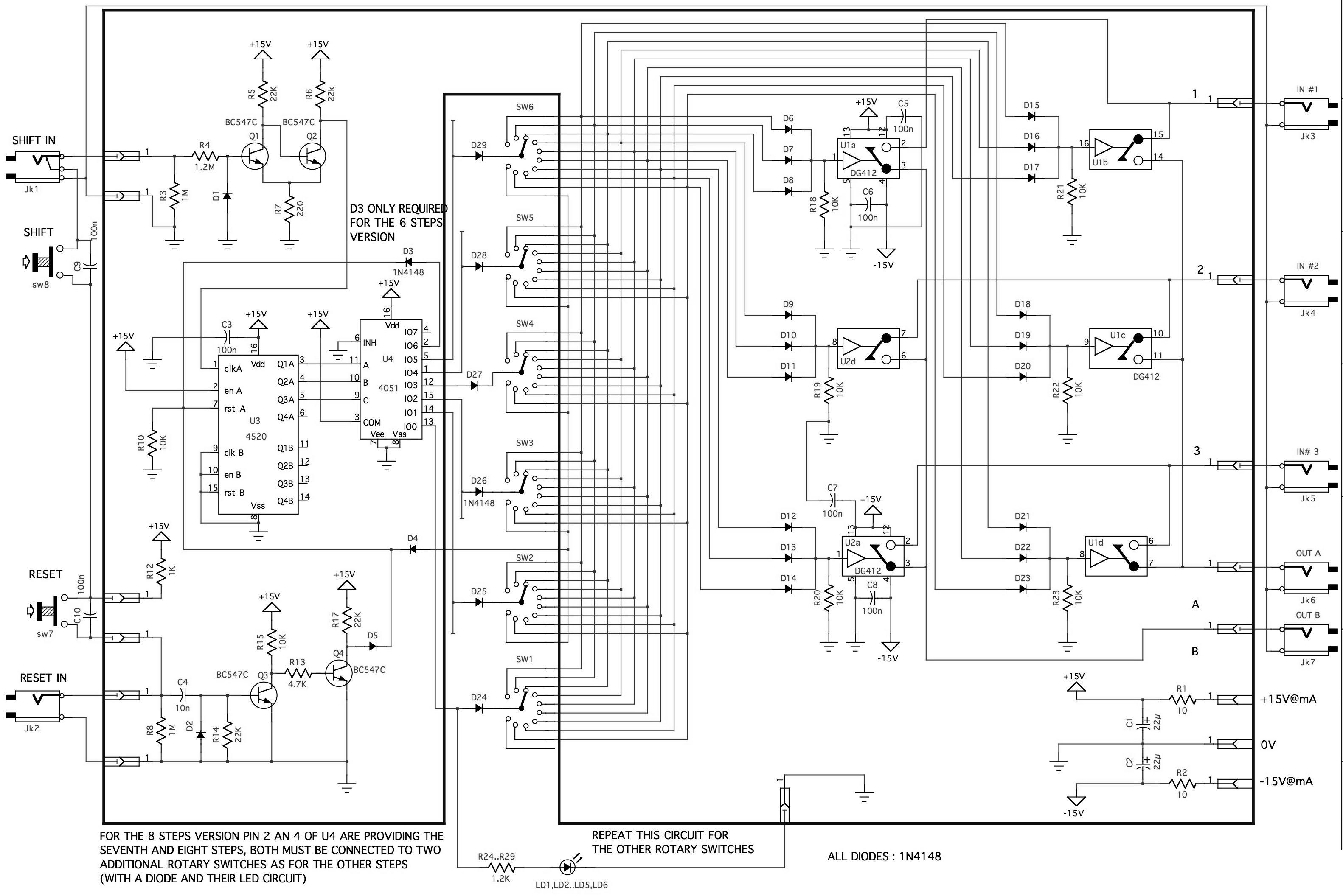
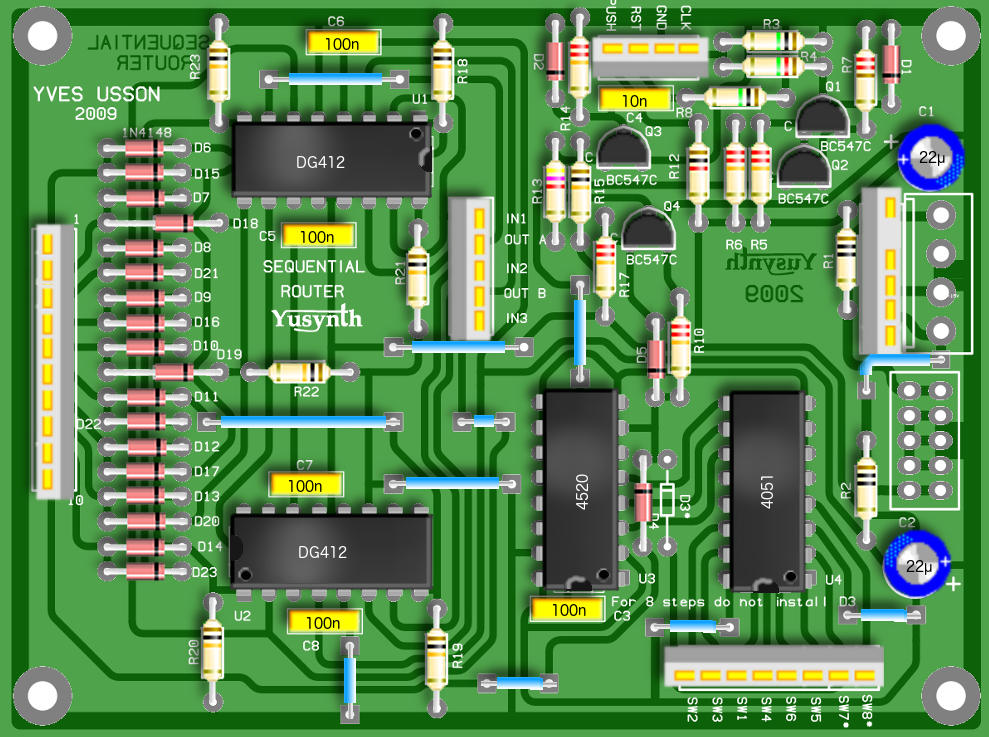
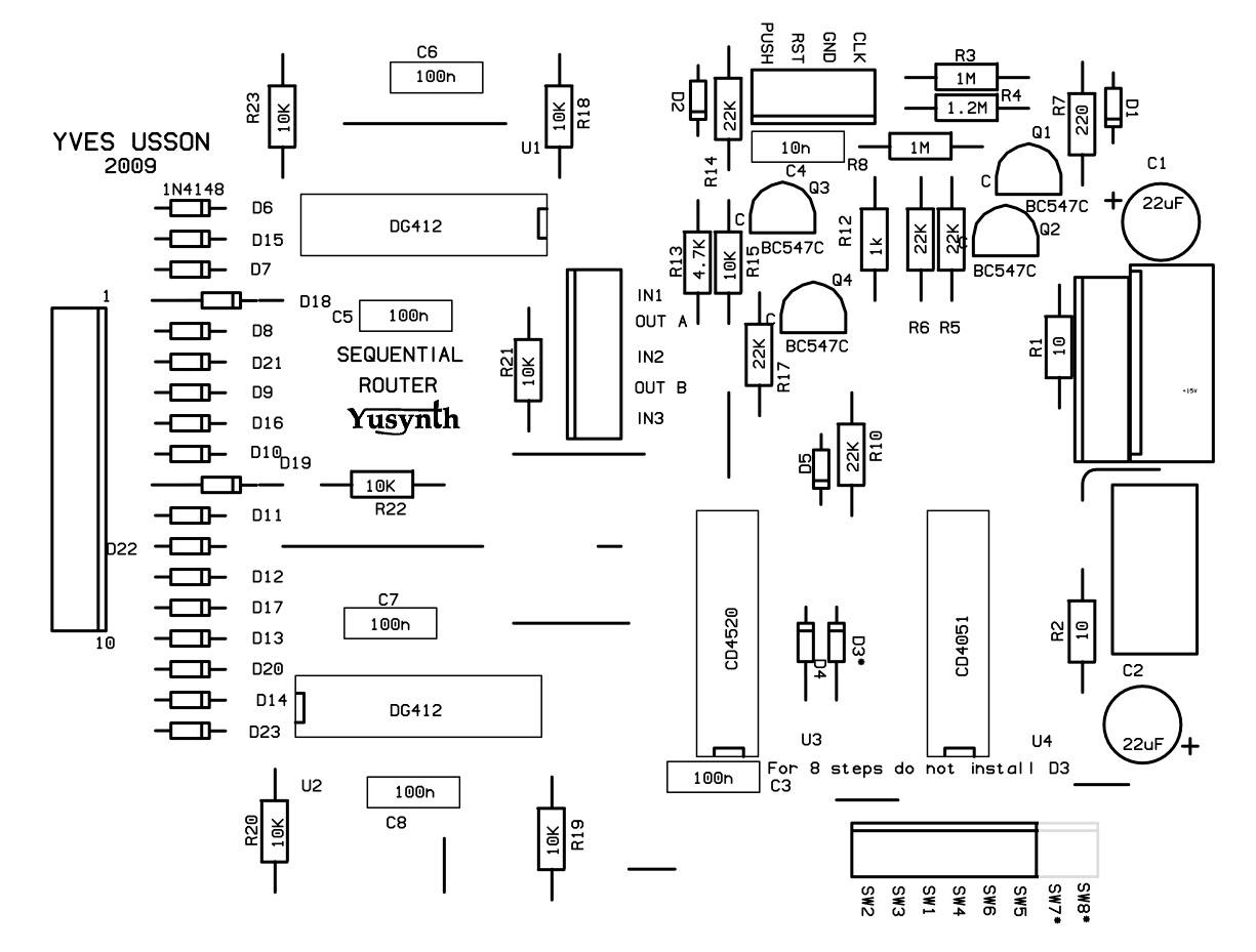
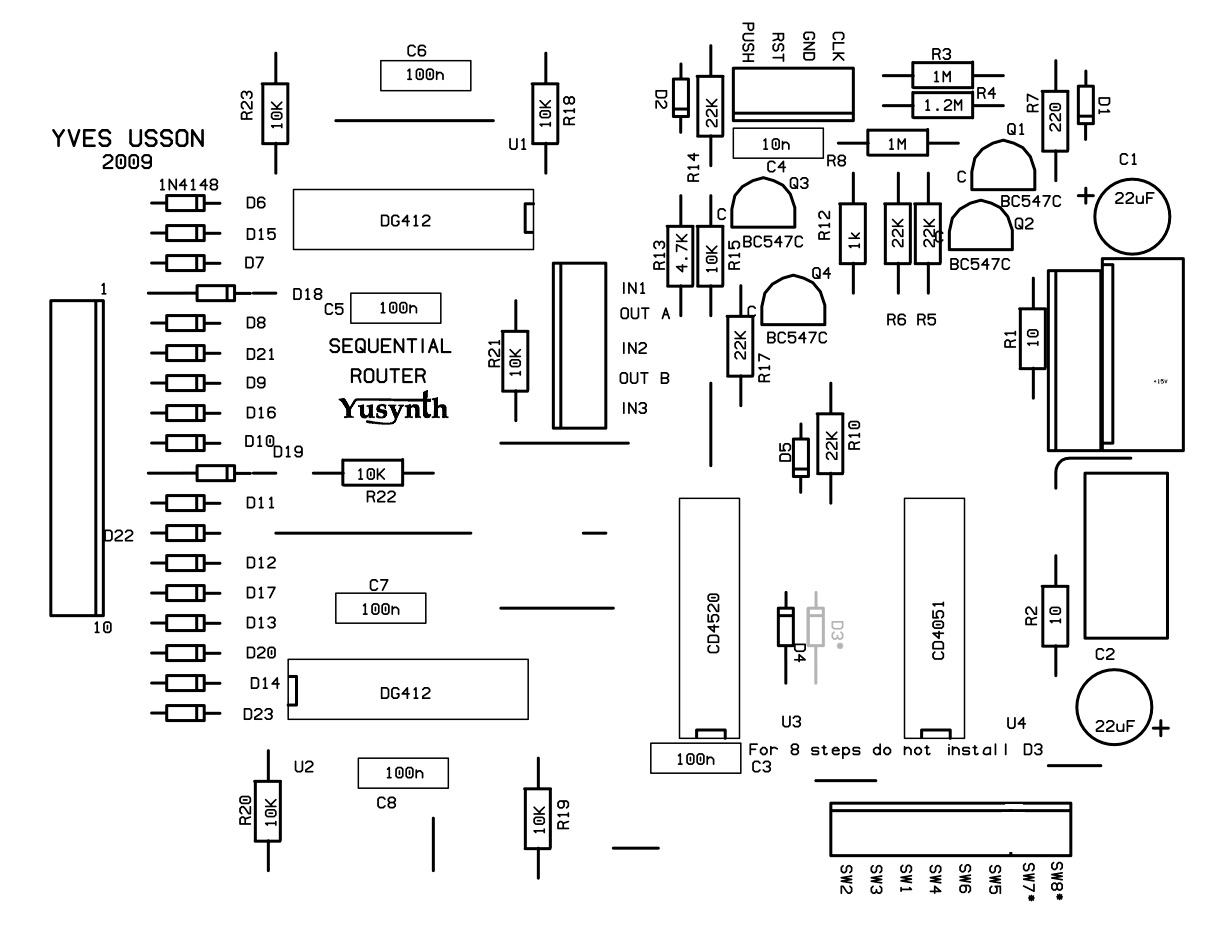
Schematic |
 |
|
Q1 and Q2 constitute a Schmitt
trigger that shapes the input pulse in order to clock a
4520 binary
ripple counter. The first three bits of this counter are
used to
address a 4051 analogue multiplexer. The output 6 of the
4051 is used
to reset the ripple counter such that the maximum number
of steps is
limited to 6. The outputs 0 to 5 of the 4051 are sent to
the rotary
switches which address a matrix of diodes forming OR
logical gates that
control six analogue switches (DG412). Q3 and Q4
provides the circuitry
for external reset.
|
|
|
| , |
|
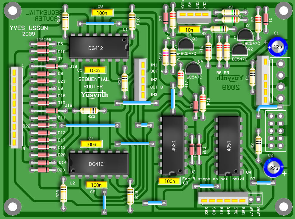
List of parts and building instructions
|
|||||||||||||||||||||||||||||||||||||||||||||||||||||||||||||||||||||
|
|||||||||||||||||||||||||||||||||||||||||||||||||||||||||||||||||||||
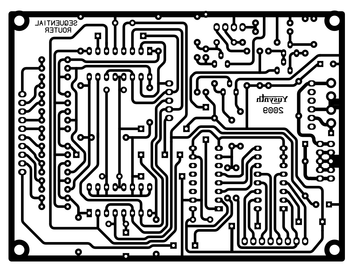
| Wiring |
|||||||||||||||||||||||||||||||||||||||||||||||||||||||||||||||||||||
|
|
|
|
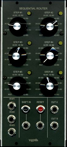
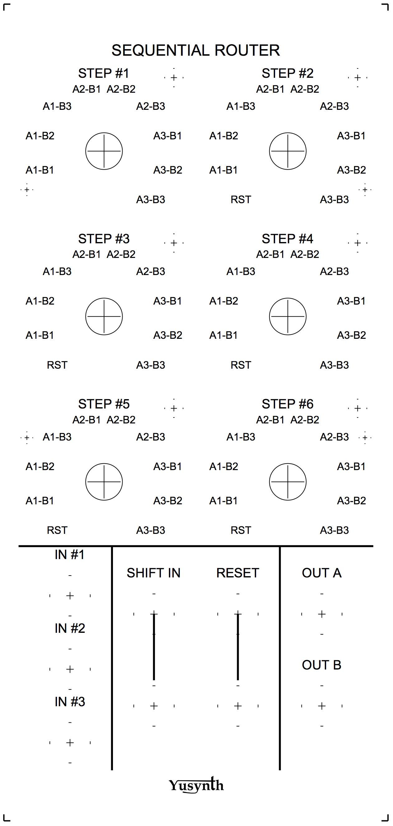
| Front plate |
||
|
|
|
Trimming
|
| No trimming is required |
|
|
|
|||
|
|
