| Modified : sep. 30th. 2017 |
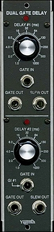
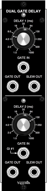
Dual GATE DELAY
|
En
français
 |
 |
back to summary |
 |
 |
| Description |
| Modified : sep. 30th. 2017 |
Dual GATE DELAY
|
En
français
|
|
back to summary |
|
|
| Description |
|
|
|
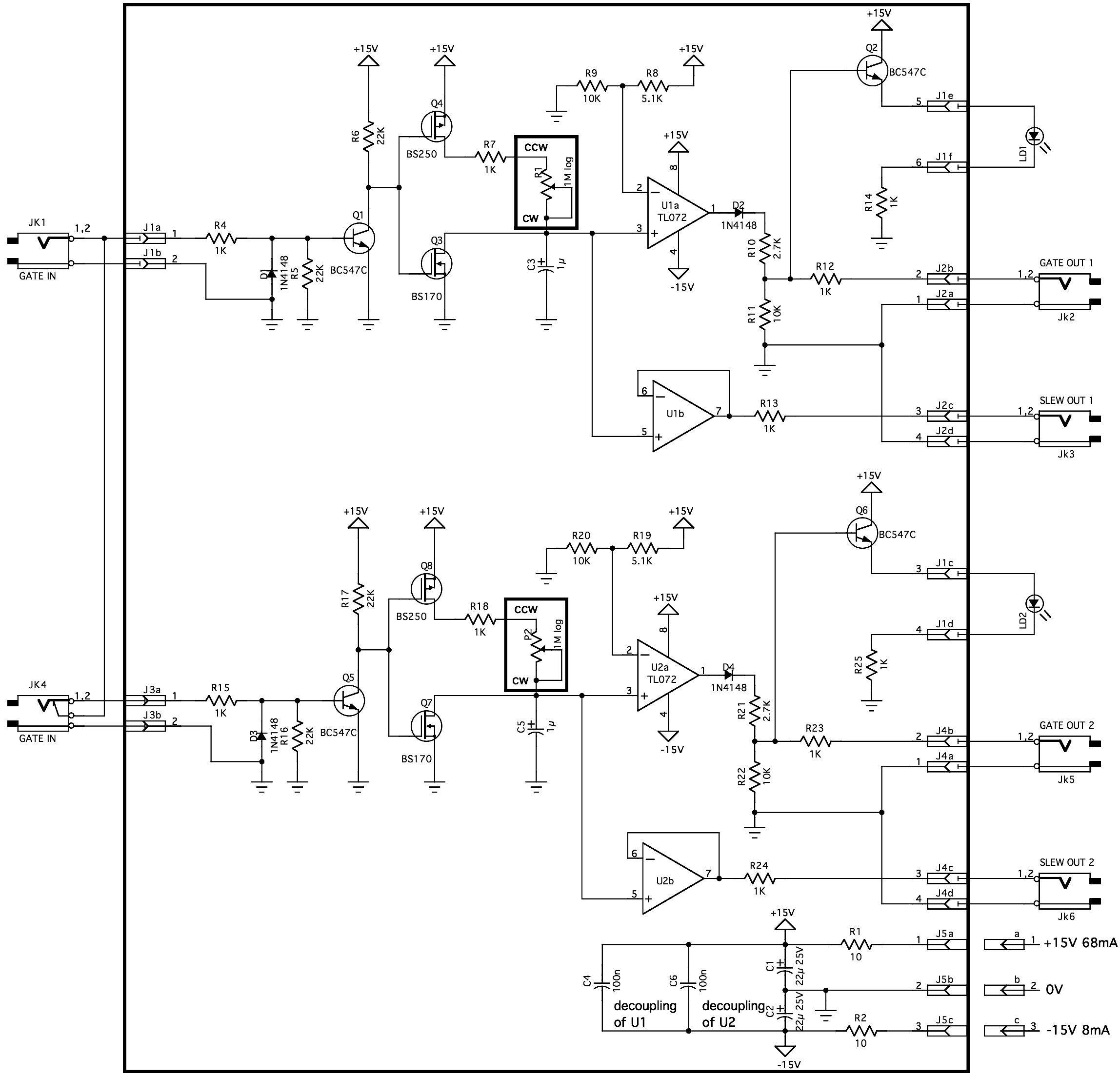
Schematic |
 |
|
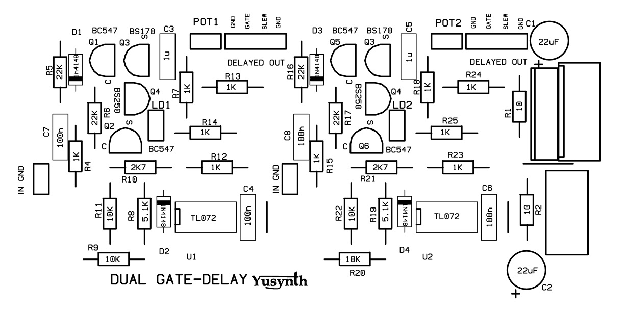
How this circuit works is quite
simple. Diode D1 protects the inputs from negative
voltage. When no
GATE signal is there, Q1 is not conducting and the gates
of Q3 and Q4
are maintained at a positive voltage (+15V).
In such a case, Q3 (N-MOSFET) is conducting and maintains C3 at a potential of 0V, Q4 (P-MOSFET) is not conducting. The U1b OPA is a voltage follower buffer and the output SLEW voltage is at 0V. The U1a OPA is acting as a comparator, the voltage at pin 3 is smaller than the voltage (+10V) at pin 2, the output GATE OUT remains at 0V. When a GATE signal (>2V) is applied to the GATE input, Q1 becomes saturated and the voltage applied to the gates of Q3 and Q4 is close to 0V. Q3 switches off while Q4 switches on. Therefore, C3 starts to charge itself at a rate depending on the sum of R7 and P1. With the values selected for R7 and P1 the charging time varies from 1ms to 1s . The output level of the comparator U1a stays at -15V as long as the voltage at C3 is smaller than 10V, the diode D1 blocks this negative voltage and the GATE OUT stays at 0V. When the voltage at C3 reaches 10V it toggles the comparator and its output becomes +15V. R10 and R11 are mounted as a voltage divisor (2/3) and the GATE OUT signal is limited to 10V. When the GATE input signals returns to 0V, the status of Q3 and Q4 is toggled and C3 is discharged very rapidly through Q3. All outputs return to 0V. Transistor Q2 is connected to the output of the comparator and drives a red LED. |
|
|
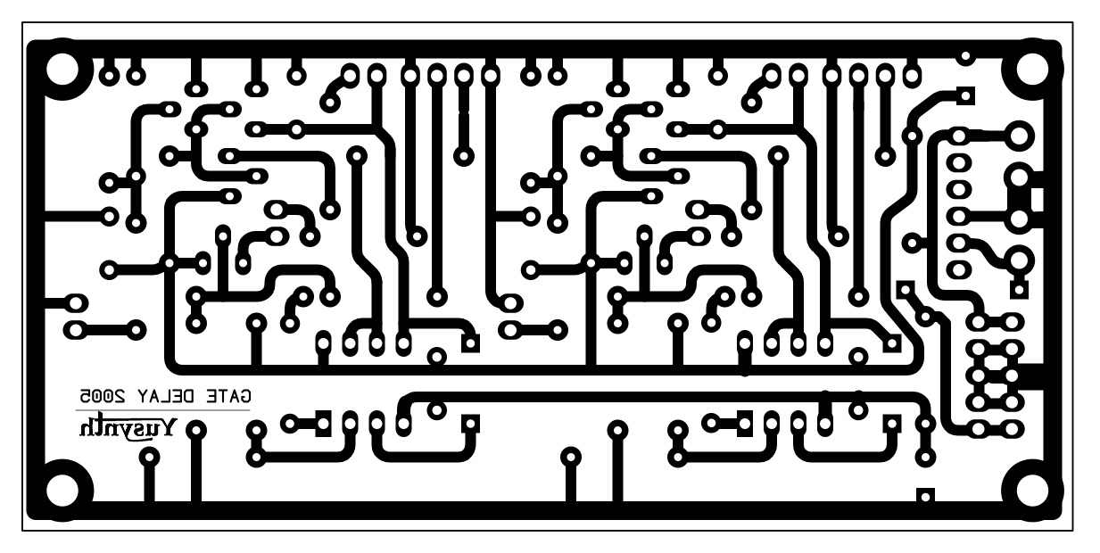
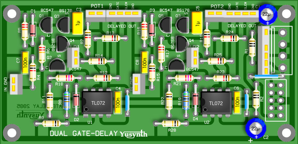
Printed Circuit Board and Component Layout
|
|||
|
|
|
List of parts and building instructions
|
||||||||||||||||||||||||||||||||||||||||||||||||||||||
|
||||||||||||||||||||||||||||||||||||||||||||||||||||||
| Note that there is no R3... |
||||||||||||||||||||||||||||||||||||||||||||||||||||||
| Wiring |
||||||||||||||||||||||||||||||||||||||||||||||||||||||
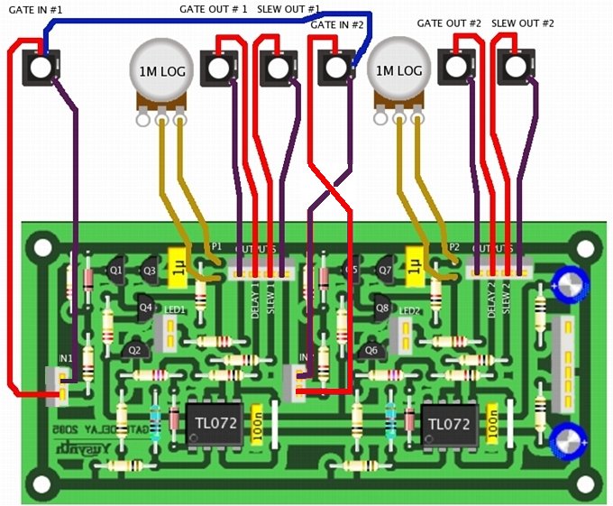 Note that the wiring of the LEDs is not shown. |
|
|
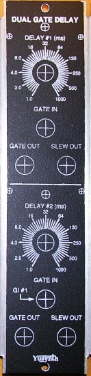
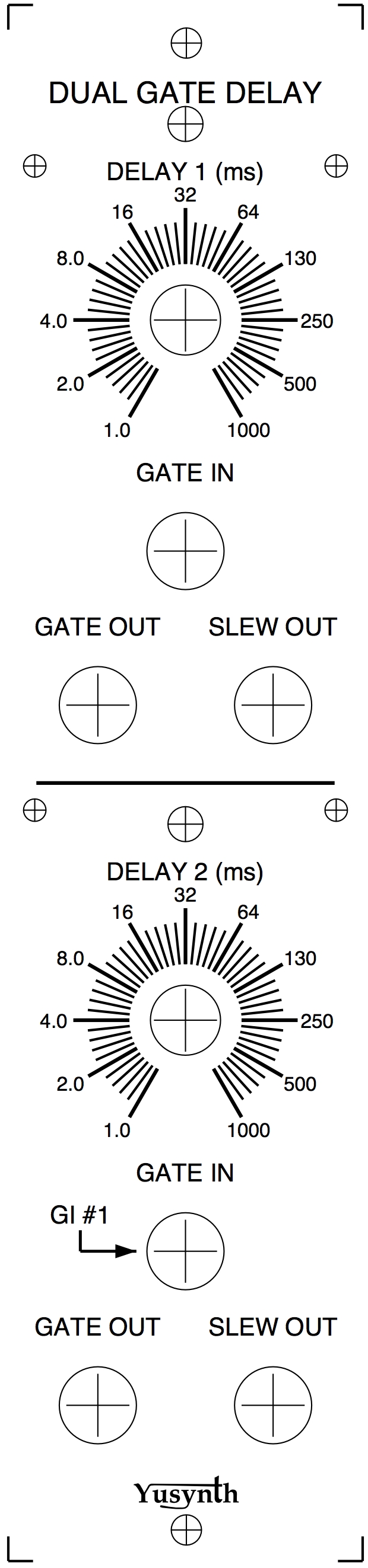
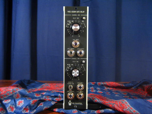
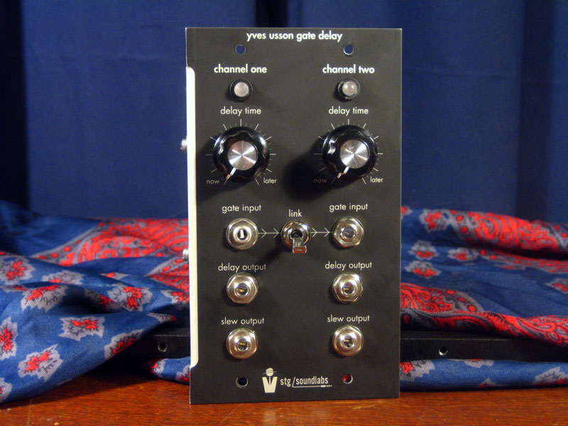
| Front plate |
|||
|
|
|
Trimming
|
| This circuit requires
no setting
or trimming. It must work right away. |
|
|
References |
Information and
datasheet for
BS170  Information and datasheet for BS250 |
  |
||
| Name : Suit
and Tie Guy Modular project : STG Soundlab Location : Chillicothe, USA Website : http://stgsoundlabs.com/ STG builds and sells a small series of this module with my agreement. |
|
|||
|
|