| Update : dec. 4th, 2018 |
Simple VCA
|
En français
 |
 |
back to summary |
 |
 |
| Description |
| Update : dec. 4th, 2018 |
Simple VCA
|
En français
|
|
back to summary |
|
|
| Description |
|
|
|
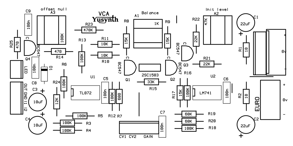
Schematics |
 |
|
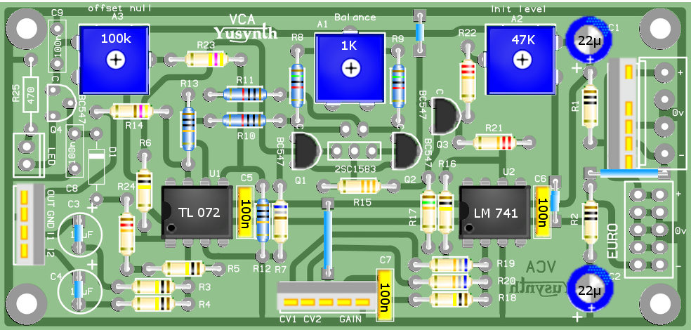
The schematic is rather simple.
U1a (1/2 TL072) sums up and inverts the two inputs. Q1 and Q2 are connected as a differential stage, it is a good practice to have these two trannies matched or to use a dual transistor such as a 2SC1583. U1b (1/2 TL072) is used as a differential unit gain "amplifier". Voltage control of the circuit is based around U2 and Q3. U2 inverts the positive voltage control, this may seem weird but is justified by the way Q3 is connected. The collector of Q3 is grounded and its emitter is connected to -15V through R19, therefore the base of Q3 must be driven by a negative bias. Q3 is current generator that forces the current through R17 which acts as a current sink for Q1 & Q2. Two versions of this circuit can be built :
|
|
|
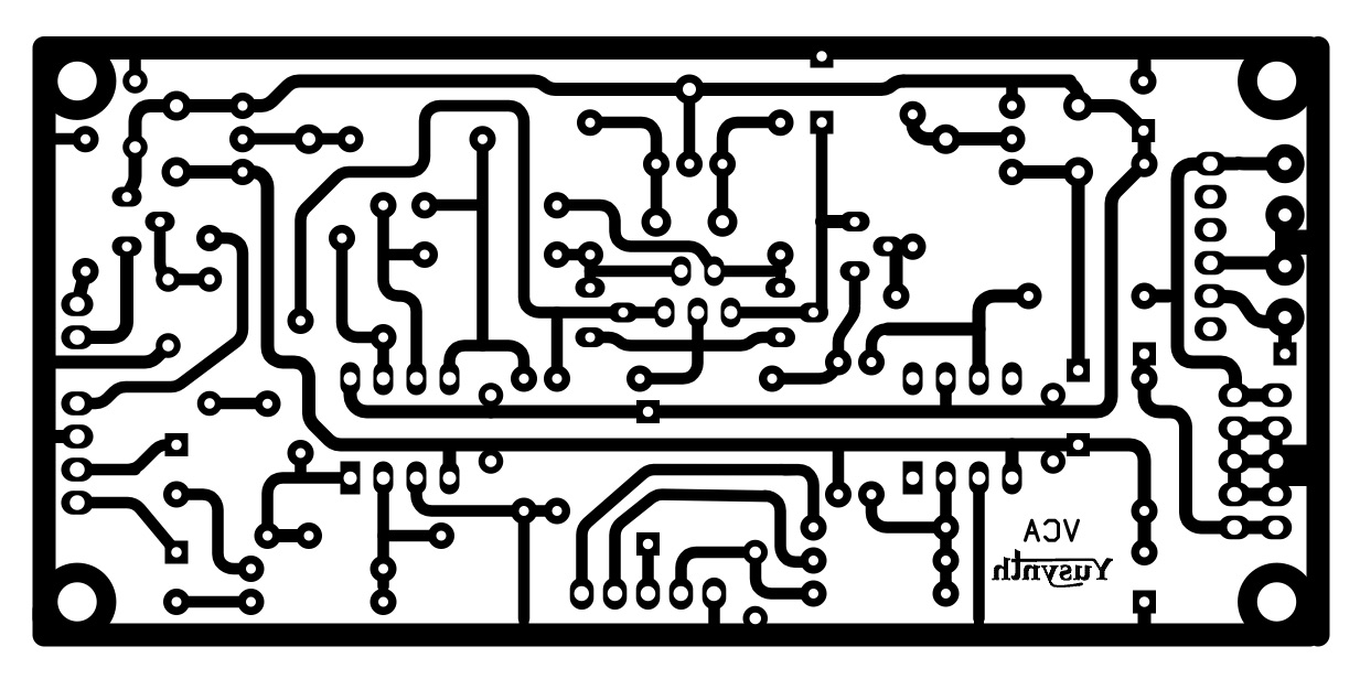
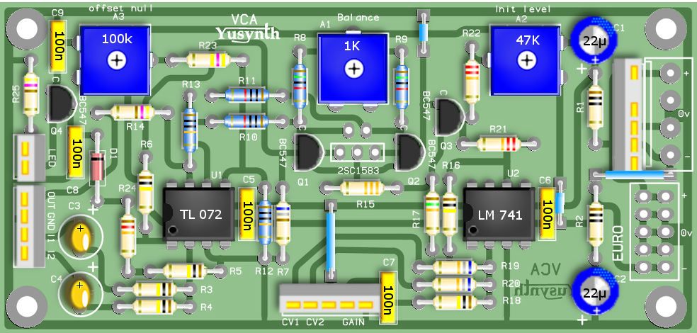
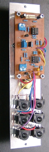
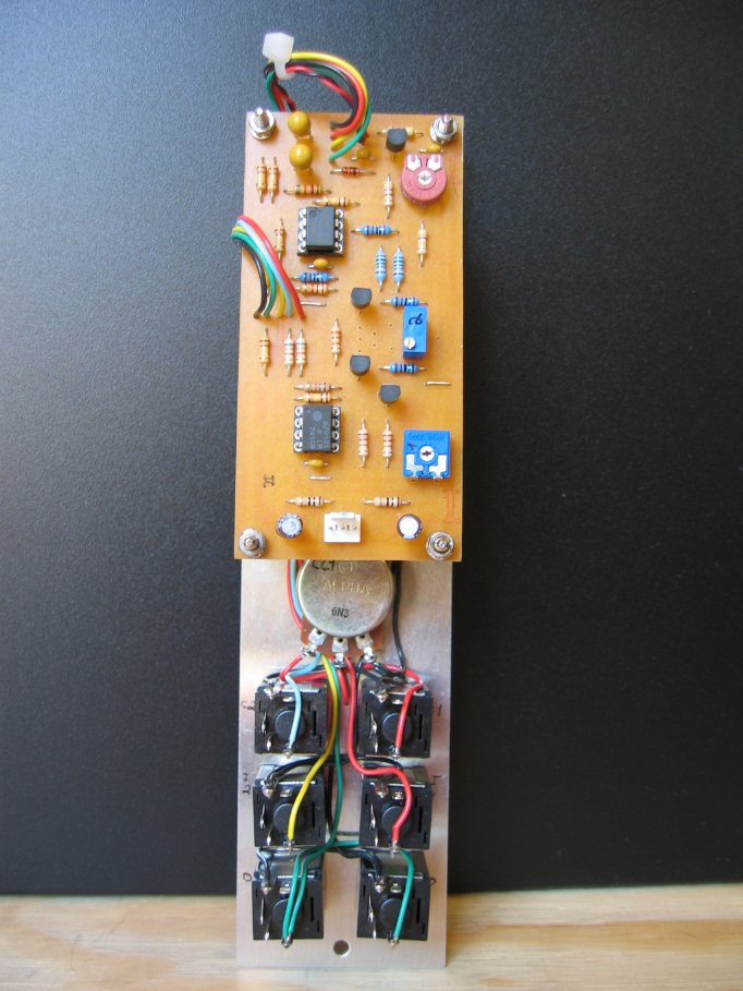
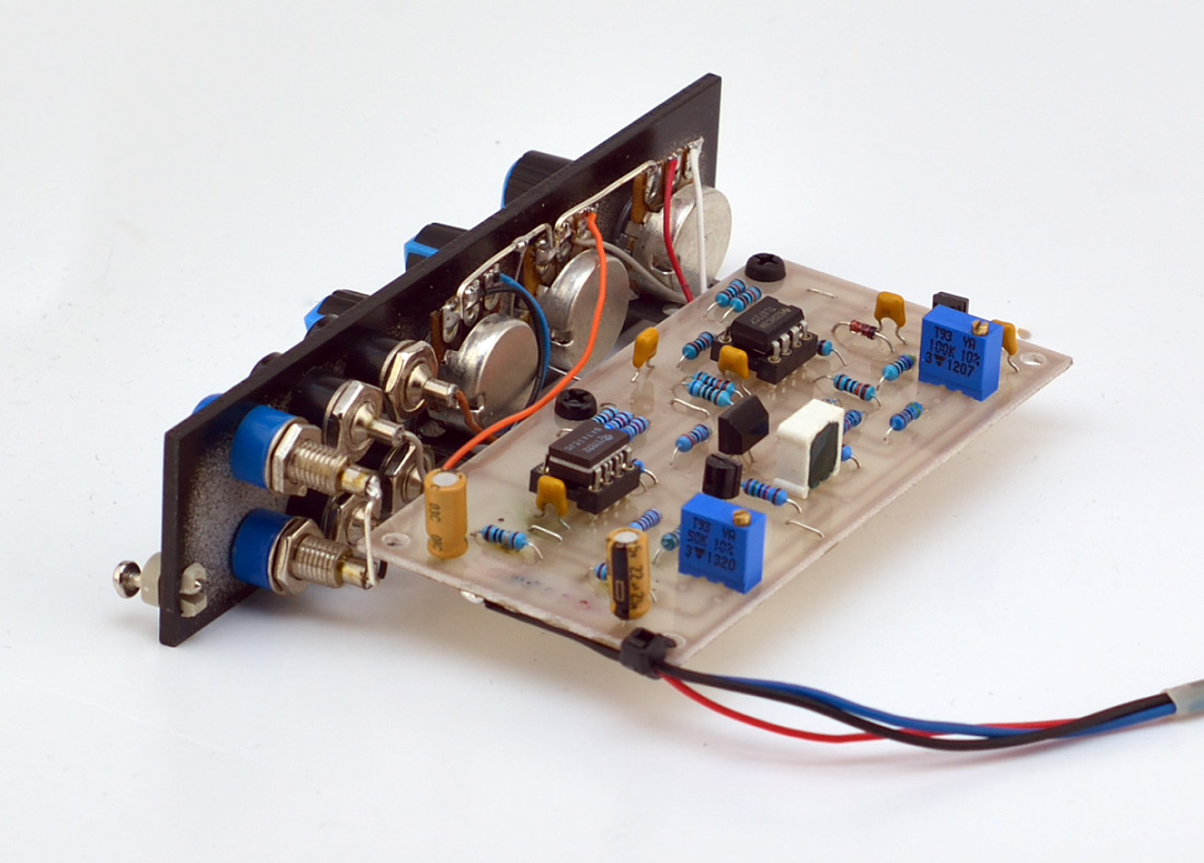
Printed circuit boards and component layout |
|||
|
|
|
Components and building details |
||||||||||||||||||||||||||||||||||||||||||||||||||||||||||||||||||||||||||||||||||||
|
||||||||||||||||||||||||||||||||||||||||||||||||||||||||||||||||||||||||||||||||||||
|
Depending on the VCA
type (AC or DC), some components are either or not
required (check the *,**).
You may also use
2N3904 for Q1, Q2 and Q3. In such a case, the pinout
of the transistors is reversed, be sure to rotate
them by 180° (flat side of Q1 and Q2 facing the
power connector J3 and flat side of Q3 facing U2) .
The LED based input level indicator circuit may be omitted if current consumption is an issue. Don't forget to solder the three straps
|
||||||||||||||||||||||||||||||||||||||||||||||||||||||||||||||||||||||||||||||||||||
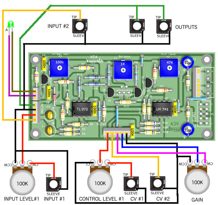
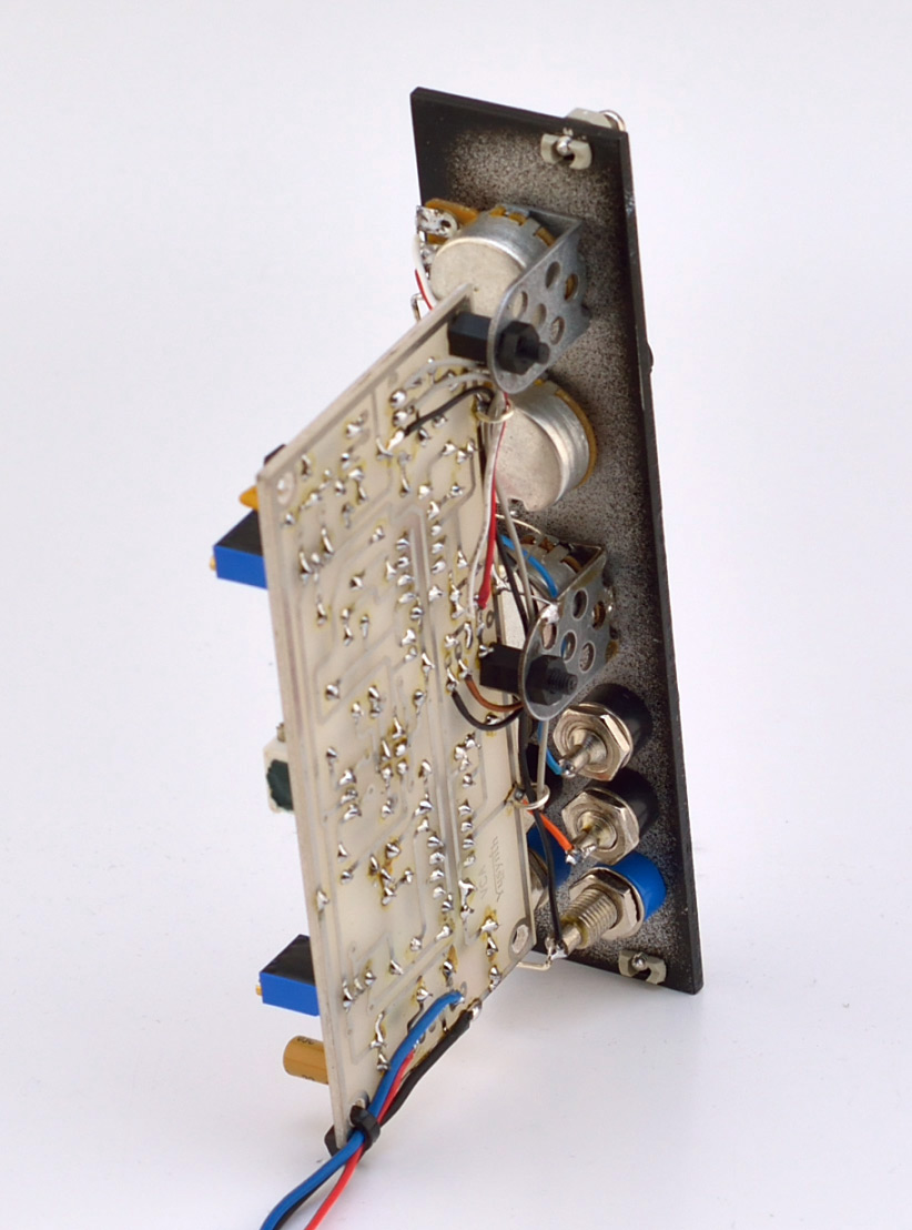
| Wiring |
||||||||||||||||||||||||||||||||||||||||||||||||||||||||||||||||||||||||||||||||||||
 |
|
|
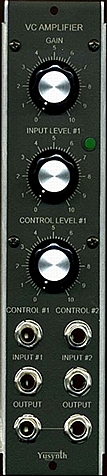
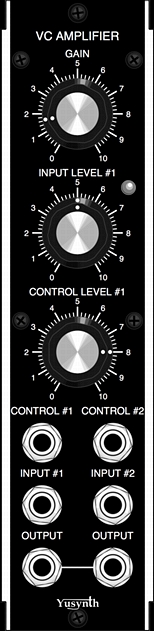
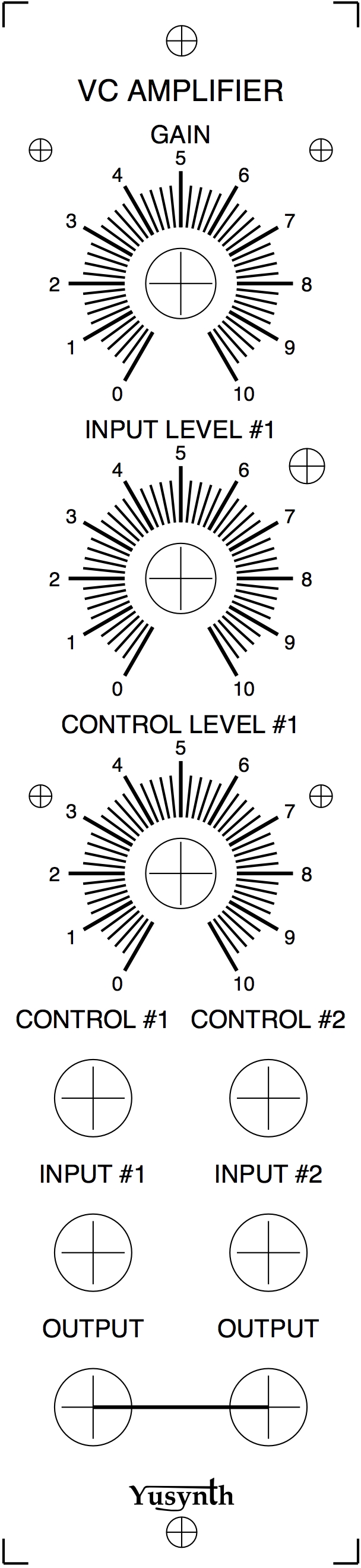
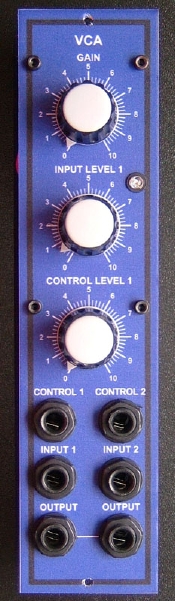
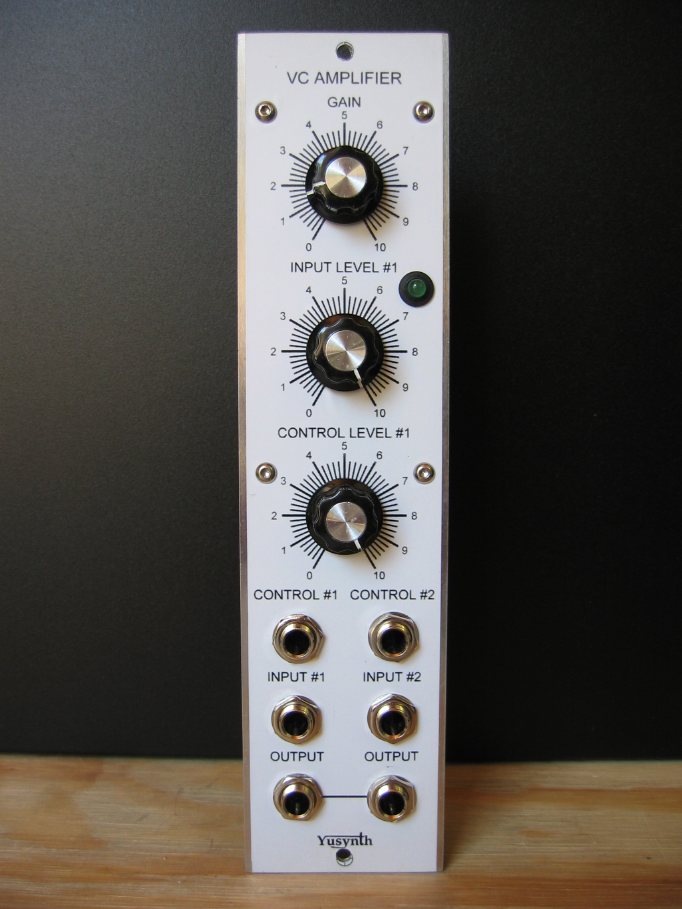
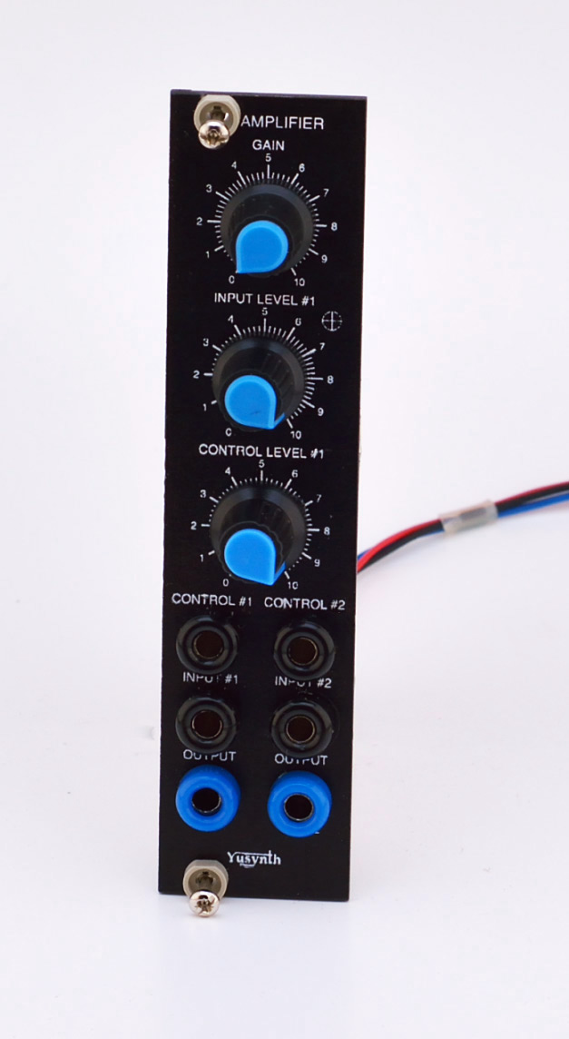
| Front panel |
|||
|
|
|
Setting and trimming
|
|
Trimming is quite
easy if you use matched NPNs for Q1 and Q2, and 1%
tolerance resistors for R6 to R11. You will need a
dual trace scope, a DVM and a sinewave generator.
Using 10 turn trimmers is a little bit more
expensive than using 1 turn but makes it easier to
adjust with high accuracy.
When used, A3 must
be adjusted as follows : after completion of
the previous settings, turn P1, P2 and P3 fully
counter-clockwise (no signal, no CV) adjust A3 in
order to have an output level (pin 7 -U1b) as close
as possible to 0V. If necessary, repeat the settings
from 2 to 7.
If you find that a unit gain for maximum control voltage is not enough for you may increase the values of R10 and R11 (e.g. setting R10 & R11 to 47K will double the output gain). Linearity versus overdrive With the component
values that are used, the VCA is perfectly linear
for input signals that do not exceed 10Vpp. Above
this level the VCA gets progressively overdriven and
starts distorting. I choose not to troubleshoot this
since overdriving a VCA can add some byte to its
sound ! On some signals (saw, square) there may be
some high frequency resonance on very steep edges,
this may be eliminated by soldering a small 7pF to
10pF ceramic capacitor in parallel with R11.
|
|
|
References |
| Actually I have
no references for this circuit ! I lost it
about 25 years ago... Here is an interesting page dedicated to Gilbert cells and balanced modulator schematics. It deserves being checked  |
The
DIY builders' gallery |
  |
  |
| Name :
Patrick Pseudo : Baronrouge Modular project: JHC live lab Location Toulon, France Web site : http://myspace.com/patjhc |
Name : Pseudo : Sebo Modular project : Location : Argentina Website : http://www.cosaquitosenglobo.com.ar |
Name : Zarko
Modular project : Location : Gardanne, France Website : |
   |
||
| Name :
Peter Hostermann Modular project : Location : Germany Website : http://www.peter-hostermann.de |
|
|||
|
|