| Modified : june. 6th. 200ç |
Octal Random Gates
|
En
français
 |
 |
back to summary |
 |
 |
| Description |
| Modified : june. 6th. 200ç |
Octal Random Gates
|
En
français
|
|
back to summary |
|
|
| Description |
|
|
|
Schematic |
 |
|
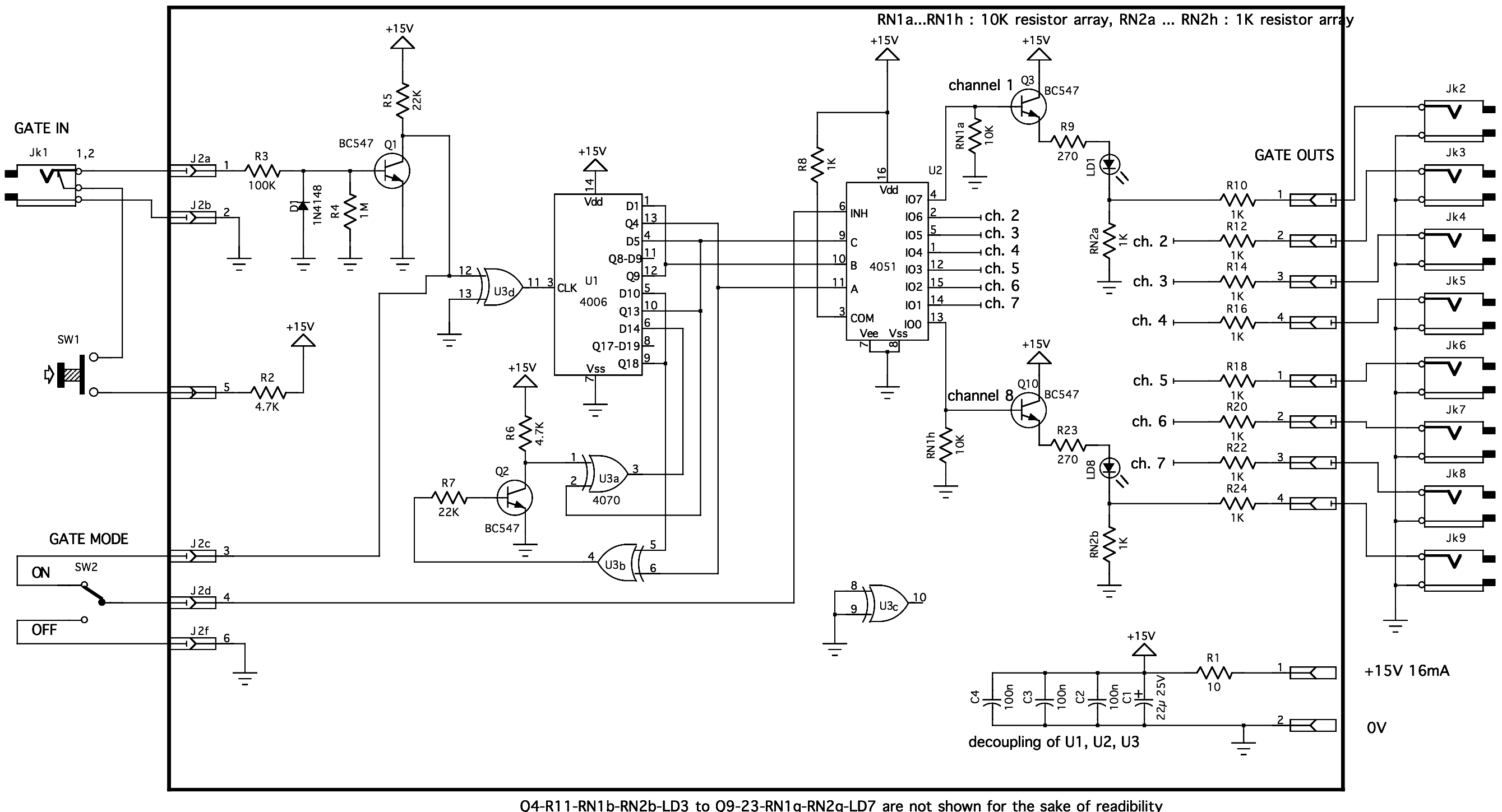
Basically, the circuit contains three
main parts : the clock input built with Q1, the pseudo random sequence
generator built with Q2, U1 and U3; and the addressing and output
stages built with U2 and Q3 to Q10.
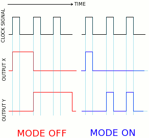
The core of the module is the pseudo-random sequence generator, it is in fact a classical circuit (Elektor) uses to generate digital noise. The CD4006 is an eigtheen stage shift register whose some of its outputs are fedback to its input through XOR gates (CD4070). Q2 inverses one of the output before applying to the XOR gate input in order to avoid an all zero status that would block the generator. The random generator is clocked by an external signal which is buffered by Q1, then a XOR gate of U3d is used to straighten the edges of the clock pulses : this was necessary to make this circuit work with some brands of the 4006 (HEF4006,MC14006) which required more stringent pulse conditions. Three outputs of the CD4006 are connected to the binary addressing pins (A,B,C) of the CD4051 (8 voice analogue multiplexer). The common pin of the CD4051 is connected to the positive rail through a 1K resistor, and all the outputs are connected to an output buffer stage. The GATE MODE switch controls the INHIBIT pin of the CD4051, in the OFF mode the INHIBIT pin is connected to the ground and the active output of the CD4051 remains active. In the ON mode the clock signal is routed to the INHIBIT pin and gates the active output. NOTE : after powering up, the module needs at least ten clock cycles before it gets into the expected behaviour. |
|
|
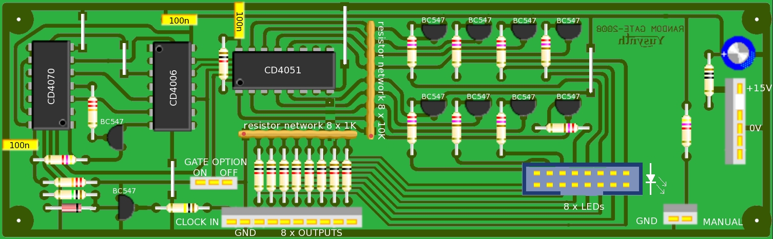
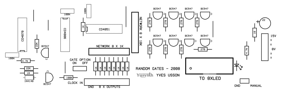
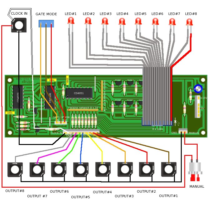
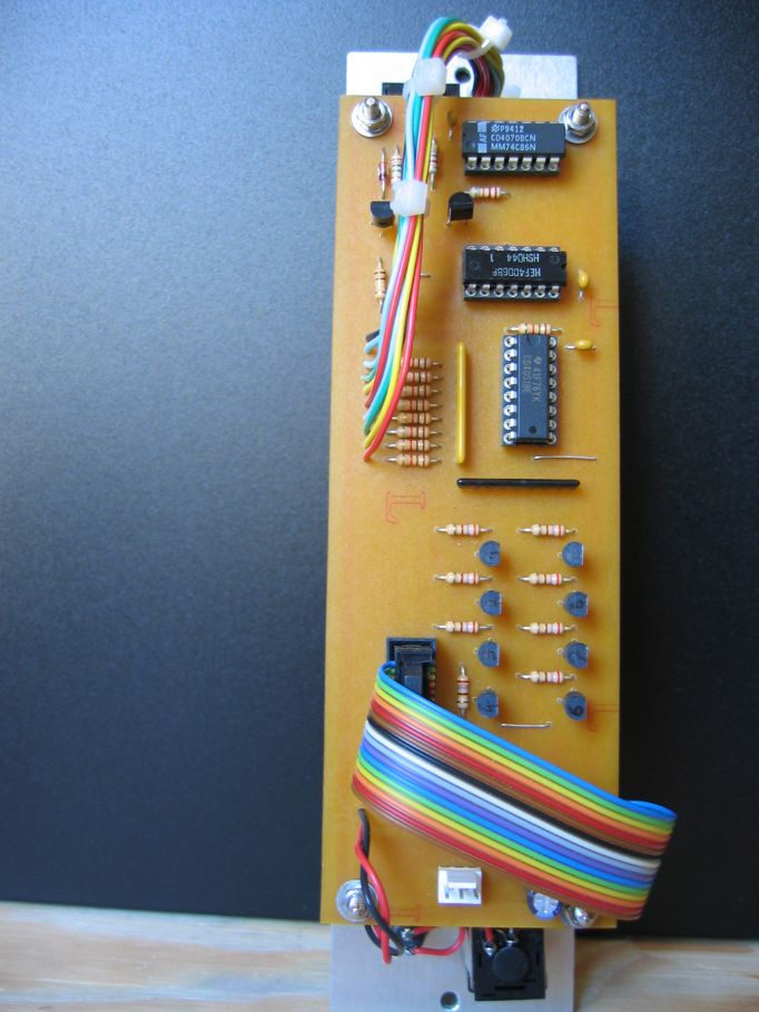
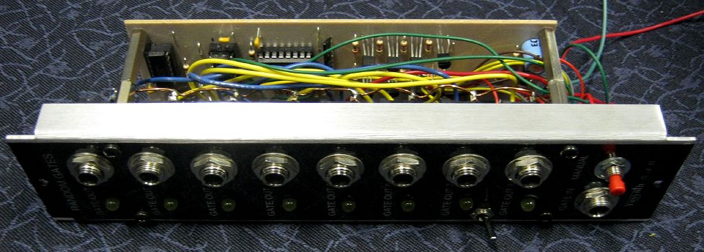
Printed Circuit Board and Component Layout |
|||
IMPORTANT NOTE : Don't forget the five straps. Also
because some tracks are quite thin and located very close to each
others, check thoroughly the PCB tracks with a looking glass in order
to detect the possible copper micro-bridges (ill-etching) and track
micro-cuts.
|
| , |
|
List of parts and building instructions
|
|||||||||||||||||||||||||||||||||||||||||||||||||||||||||||||||||||||
|
|||||||||||||||||||||||||||||||||||||||||||||||||||||||||||||||||||||
| Wiring |
|||||||||||||||||||||||||||||||||||||||||||||||||||||||||||||||||||||
 |
|
|
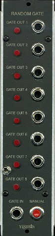
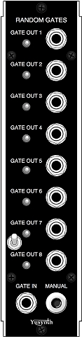
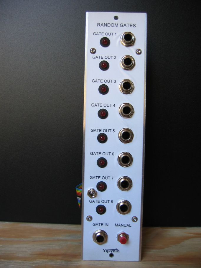
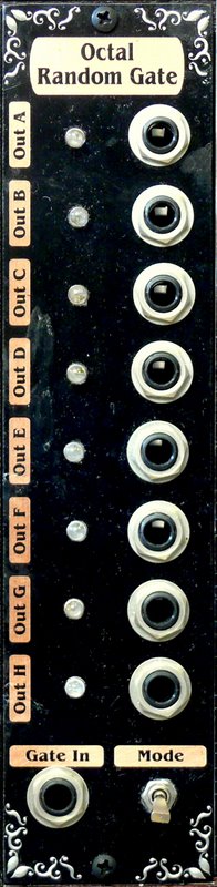
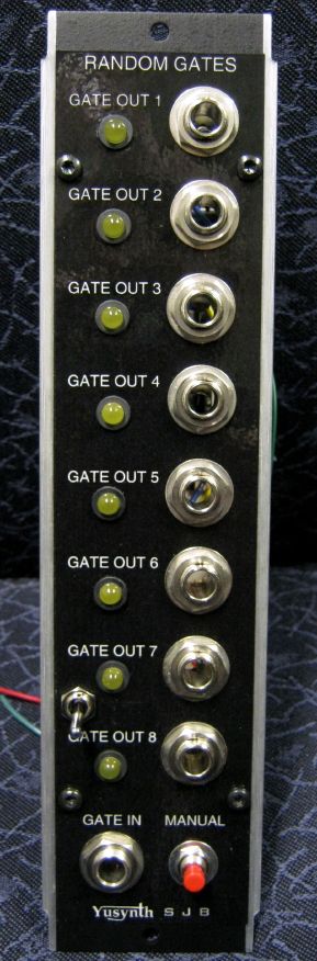
| Front plate |
||
|
|
|
Trimming
|
| This circuit requires no
trimming. It must work when powered on. NOTE : after powering up, the module needs at least ten clock cycles before it gets into the expected behaviour. |
|
|
Modifications of the old PCB
|
NOTE : these modifications are only
for those who built the circuit with the old PCB
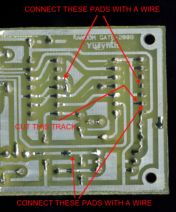
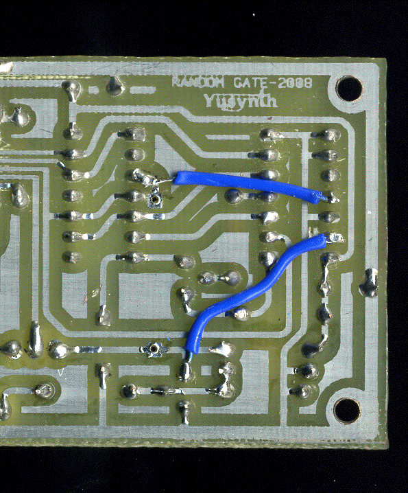 Remove the long strap between the
collector of Q1 (lowest transistor on the layout) and pin 3 of U1
(4006).
With an sharp knife cut the short track from pad 13 of U3 (4070), connect a short isolated wire between pad 11 of U3 and pad 3 of U1, connect a short isolated wire between pad 13 of U3 and the collector of Q1. |
|
|
  |
 |
  |
| Name
: Frédéric Monti Pseudo : Zarko Modular project : Location : Gardanne, France Website : |
Name
: Doug Slocum Pseudo : Modular project : SteamPunk Location : USA Website : www.dougslocum.com |
Name
: Steven Brenner Pseudo : Modular project : Location : Waterloo, Ontario, Canada Website : |
|
|||
|
|