| Update : jan. 31st, 2009 |
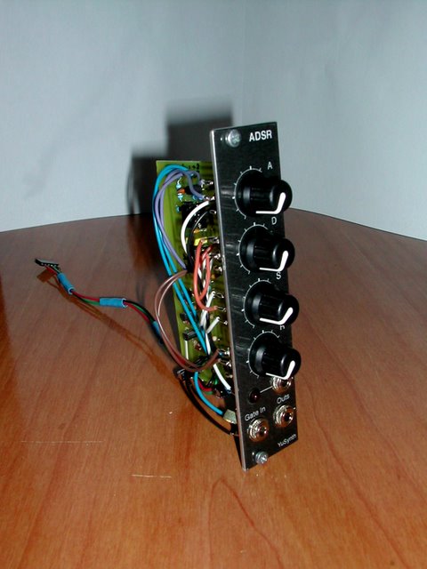
Envelope generator
ADSR |
En
français
 |
 |
back to summary |
 |
 |
| Description |
| Update : jan. 31st, 2009 |
Envelope generator
ADSR |
En
français
|
|
back to summary |
|
|
| Description |
|
|
|
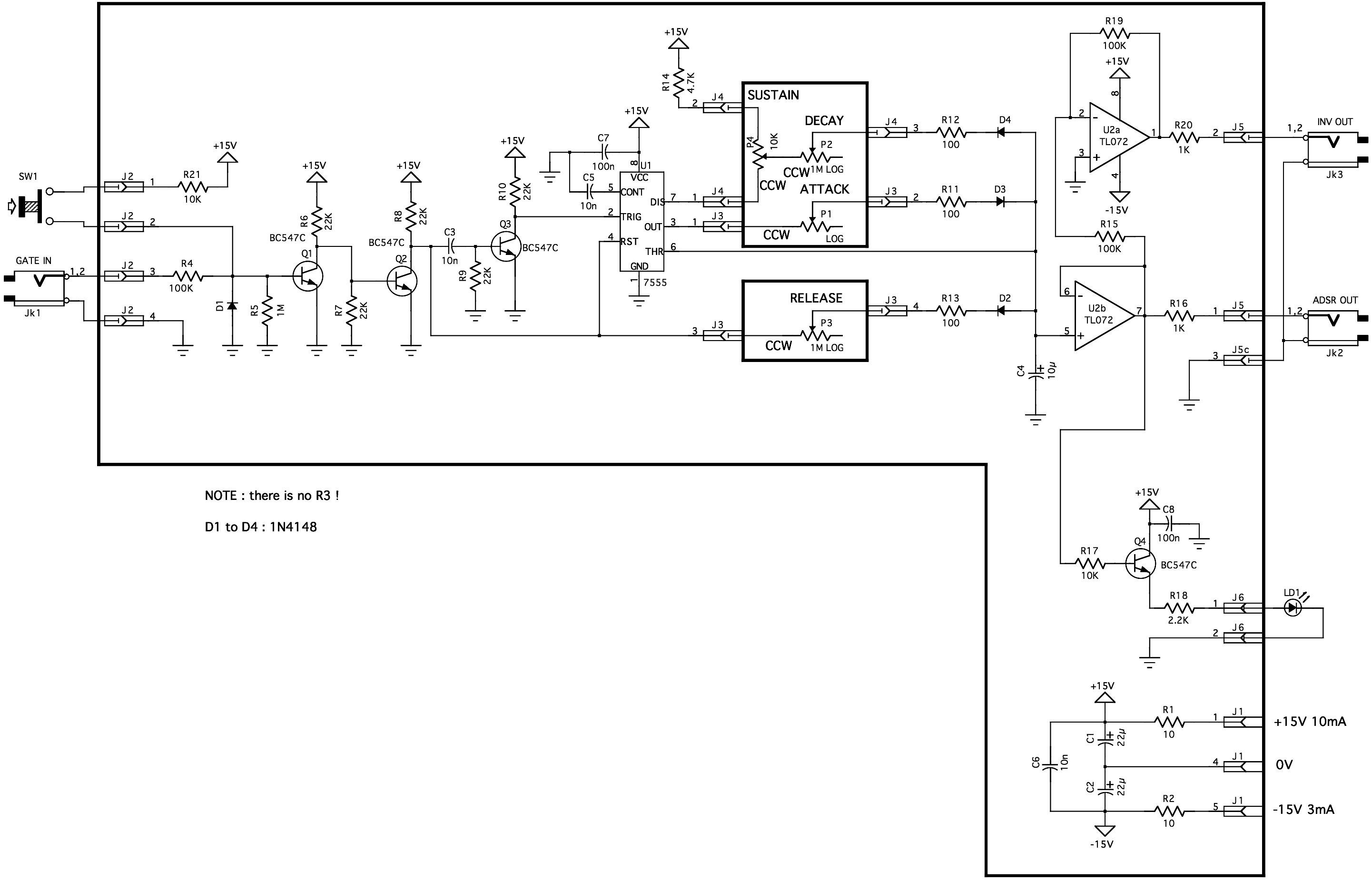
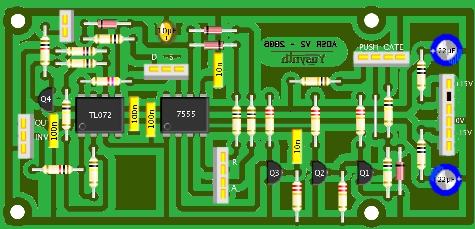
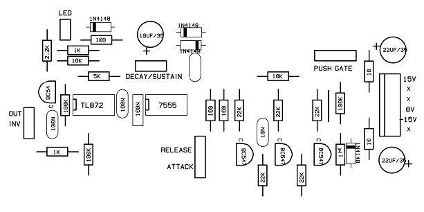
Schematic |
 |
|
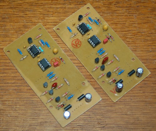
The schematic of this
module is rather simple and uses very common
components. The core of the schematic is based on an original idea by Jonathan
Jacky
 that was published in Electronics ("Two-chip
generator shapes synthesizer's sounds" Electronics #11,
September
1980 : 137-138). This core has inspired other DIYers (Tom
G.-EFM, René
Schmitz ). that was published in Electronics ("Two-chip
generator shapes synthesizer's sounds" Electronics #11,
September
1980 : 137-138). This core has inspired other DIYers (Tom
G.-EFM, René
Schmitz ). Three transistors (Q1 to Q3, BC547C) are used to process the GATE signal. D1 protects the circuit from negative voltages. Diodes D2 to D4 are used to dispatch the charge and discharge current of the timing capacity C4 (10µF/35V tantalum) through the potentiometers P1,P2 & P4. The 7555 chip (U1) is wired as a monostable timer. The two OPAs of the TL072 chip (U2) are used as a simple voltage follower and a voltage inverter, respectively. Next, transistor Q4 drives the control LED. |
|
|
| How does it work ? |
|
|
||
|
||
|
||
|
||
|
||
|
|
|
|
|
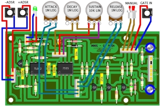
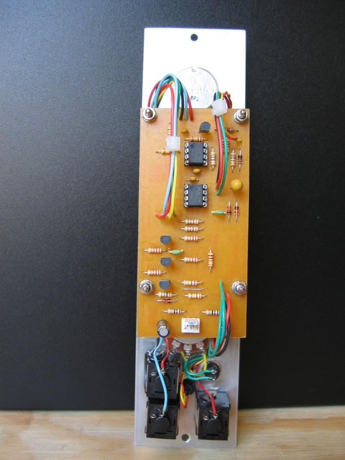
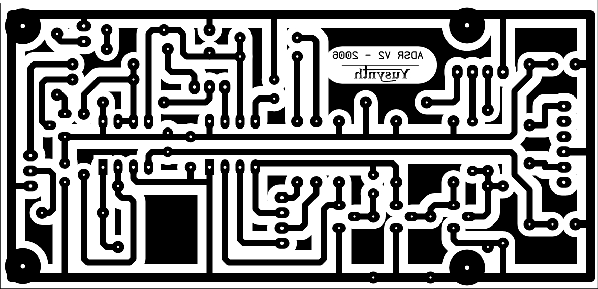
Components and building guide
|
|||||||||||||||||||||||||||||||||||||||||||||||||||||||||||||||||||||
|
|||||||||||||||||||||||||||||||||||||||||||||||||||||||||||||||||||||
| R3 is missing... |
|||||||||||||||||||||||||||||||||||||||||||||||||||||||||||||||||||||
| Wiring |
|||||||||||||||||||||||||||||||||||||||||||||||||||||||||||||||||||||
 |
|
|
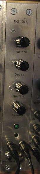
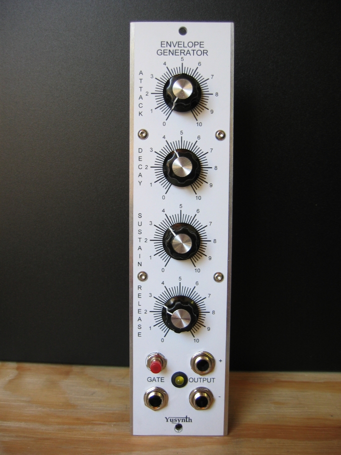
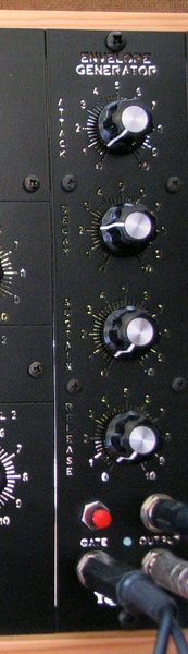
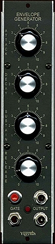
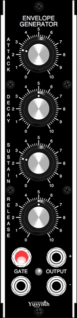
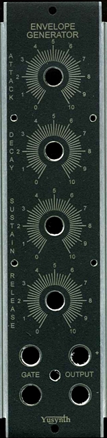
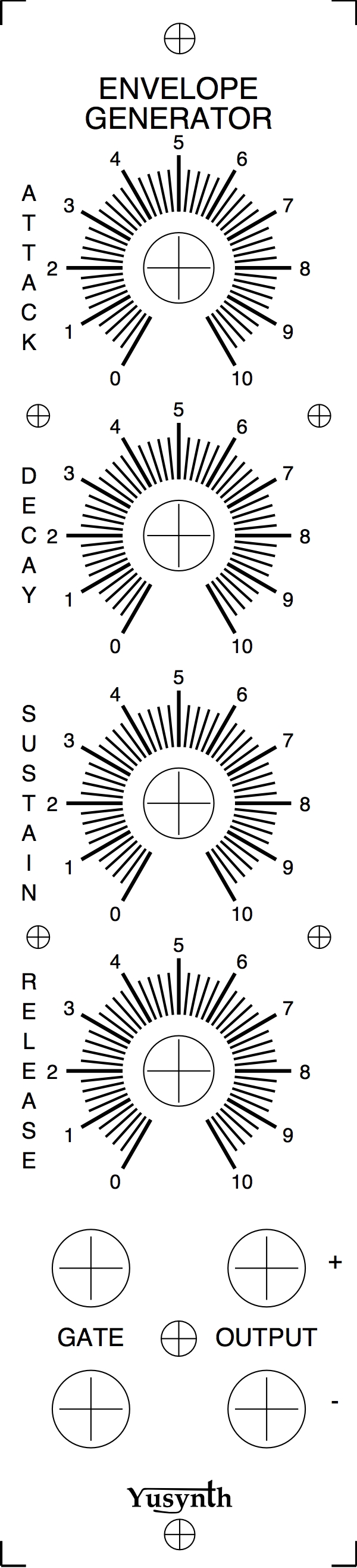
| Front panel |
|||
|
|
|
Settings and trimming
|
| This circuit does not require any trimming. |
|
|
Références |
|
 |
 |
 |
| Name
: Czaba ZVEKAN Modular project : Location : Basel, Switzerland Website : |
Name
: Etaoin Modular project : Casia MS01 Location : Utrecht, Netherlands Website :www.casia.org/modular |
|
 |
  |
 |
| Name
: Jordi Pseudo : vcfool Modular project : Location : Website : |
Name
: Pseudo : Sebo Modular project : Location : Argentina Website : www.cosaquitosenglobo.com.ar |
Name
: Doug Slocum Pseudo : Modular project : SteamPunk Location : USA Website : www.dougslocum.com |
  |
 |
 |
| Name
: Frédéric Monti Pseudo : zarko Modular project : Location : Gardanne, France Website : |
Name
: Pseudo : Tudy Modular project : Yusynth 17U Location : Brno, Czech Republic Website :www.insania.freemusic.cz |
Name
:
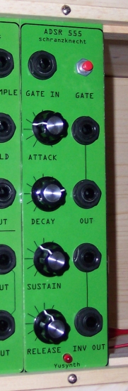
Torsten Pseudo : fogman Modular project : schranzknecht Location : Germany Website : www.vulkanware.de/diy |
|
|||
|
|
